menu
close_24px
Deep Learning For Failure Analysis & Process Engineering

Harness the Power of Computer Vision to Streamline Failure Analysis

Discover the power of uncovering minuscule imperfections in the nano world, all at lightning speed.
Even the tiniest flaws in the micro world can unleash significant complications in the larger realm of technology.

As nanotechnology, material science, and semiconductor manufacturing technologies continue to evolve, everything gets smaller. However, the nanotechnology also amplifies the impact of minor defects on semiconductors, materials, and MEMS.

Fortunately, Deep Block's cutting-edge machine vision technology, integrated with its ultra-high-resolution microscope image analysis, emerges as the ultimate solution to conquer these intricate challenges and eliminate imperfections.

Why are high-resolution images difficult to analyze?

Discover the countless challenges posed by large-volume, high-resolution images.

Discover the incredible challenges presented by large-volume, high-resolution images. These images are truly massive in terms of their size. Simply rendering high-resolution images on the front-end is a complex task, and combining such enormous images with machine vision technology poses an even greater challenge.

Due to their size and resolution, these images need to be divided and analyzed. However, this process brings a lot of problems, including speed problem and the potential loss of features when analyzing the countless pieces of the image.

Fortunately, by harnessing the power of Deep Block's computer vision technology specifically designed for ultra-high resolution images, your microscopic image analysis can be effortlessly automated, making it incredibly easy.

What We Do

Failure Analysis & Layer Morphology Analysis

While the thin film remains unseen to our unaided vision, it reveals itself as a THICK layer when magnified by an electron microscope.

We are very interested in the step coverage, morphology, and composition of each layer, but we rely on our eyes to see the thickness and connectivity of the numerous gates and metals that exist in the HUGE WAFER OCEAN.

Take control of your Micrograph analysis today without any coding knowledge. Create your own machine learning model and harness the power of our state-of-the-art machine vision technology. Trust Deep Block to gain insight into thin film morphology.

interconnect


Connectivity of Metal

Assess metal connectivity with precision. As vias diminish in size and the necessity to packaging the chip arises, it becomes crucial to consistently guarantee the process examination of both deposition and etching processes after every adjustment.

Leveraging TEM for comprehensive, destructive analysis or employing SEM for detailed surface exploration, our cutting-edge computer vision technology is at your disposal to elevate the evaluation of the expansive surface.

TSV


Through Silicon Via

Connecting chips requires precision drilling of tiny holes, a task so delicate that a single misstep makes the chips unusable.

As the complexity of this task mounts, we're faced with the challenge of creating thousands of these minuscule connections.

The nature of attaching one chip to another becomes a painful journey. And when things don't go as planned, the sting of criticism from our supervisor is followed by long nights hunched over a microscope, engaged in failure analysis to pinpoint the exact cause of the error.

Fear not, for Deep Block stands by your side, ready to alleviate the strain of this intricate process!

gaafet


Process Engineering

Ensure the precise deposition of each layer and examine the your process.

Even the smallest variation in thickness or an unforeseen etching mishap can undermine the chip manufacturing process, resulting in its failure.

With the advent of cutting-edge design like GAA, demanding the use of destructive examination to inspect them.

Embrace the power of machine learning to automatically evaluate the thickness and configuration, enhancing your quality control measures.

What We Handle

Stitched TEM, SEM

The tiny chip is TOO LARGE under the microscope.
Whether you want to cut the chip and look at its cross section, or inspect the entire surface, DEEP BLOCK's LARGE-scale image analysis technology will be of great help!

Why TEM?

The demand for Transmission Electron Microscopy (TEM) is significantly boosted by the NXE systems, packaging technologies, and High Bandwidth Memory (HBM).

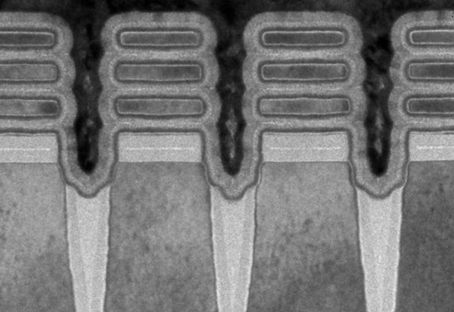
As vias and layers shrink in size, the details we need to observe become increasingly minuscule.

The limitations of in-situ imaging become apparent, necessitating destructive testing and the indispensable use of Transmission Electron Microscopy (TEM).

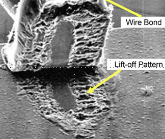
For example, SK Hynix is at the forefront with a specialized TEM team.

Your company also have own experts who prepare chip samples for TEM analysis on a daily basis.

Looking ahead, the quest to explore even finer structures means TEM will become more crucial than ever.

We are tasked with the intricate challenge of discerning the smallest of structures, interpreting very thin films as mere lines, dots, or substantial layers.

GaN


GaN

Gallium nitride wafers, although riddled with imperfections, require your keen eye for defect detection and subsequent failure analysis. Simply capture ultra-high resolution images using TEM and let the automatic analysis unveil the insight hidden within.

hybrid bonding


Packaging

Microscopes play a pivotal role in every aspect of packaging processes, encompassing techniques such as through-glass via and hybrid bonding. Tackle your failure analysis with Deep Block!

ald


Atomic Layer Deposition

Allow us to be your guide in analyzing thin-film depositions. The key to unlocking the secrets of morphology lies in the precise segmentation of layers. While the task of measuring dimensions such as length and area might seem daunting, rest assured, it becomes effortlessly straightforward with the application of computer vision technology!

THE TECH

The world's fastest imagery analysis solution.


Deep Block_the tech_max file resolution
10 GP pixels

Max file resolution
or 100,000 x 100,000 pixels images.

Deep Block_the tech_max file size
40 GB

Max file size
vs. 1 GB with our competitors.

Deep Block_the tech_processing speed
10GB/sec.

Processing
speed.

Deep Block_the tech_mAP
0.9 AP

Highly accurate prediction
when detecting objects.

Deep Block_the tech_recall
0.9 Recall

Highly reliable detection
with minimum false negatives.

ENTERPRISE FEATURES

When confidentiality and security are not only buzzwords.

At Deep Block, we understand the needs of large enterprises and public organizations and are willing to work closely with your team to ensure a smooth deployment and usage of the solution.

Deep Block Advanced Security
Advanced Security

Get additional security features to fit your compliance needs like VPN connection, monitoring, fixed IP, and others.

Deep Block Custom Domain
Custom Domain

Get your own enterprise account, allocated users seats, and branded domain.

Deep Block Self-Hosting Support
Self-Hosting Support

Host Deep Block in your own private cloud or on-premise for maximum security.

Deep Block Access Provisioning
Access Provisioning

Define user accesses and privileges to make sure that the right person has access to the right information.

Deep Block Workflow Customizations
Workflow Customization

Request custom interfaces, features, or workflows directly from our engineering team.

Deep Block Premium Support
Premium Support

Our support team will be monitoring your needs on the clock to ensure a smooth Deep Block experience.

CONTACT US

Interested? Let's get in touch!

Whether it is to get a demo of our Deep Block Platform, inquire about our learning courses, join our latest Bootcamp or explore custom solutions with us, we will be happy to help!