
Surface Mount Technology and Inspection

Surface Mount Technology (SMT) is at the heart of modern electronics manufacturing. From smartphones to satellites, nearly every electronic device we use today owes its compact size and performance to the SMT process. But what ensures this complex process results in reliable, high-quality circuit boards? The answer lies in careful quality control, repeated inspection, and sometimes, the microscopic lens.
What Is SMT?
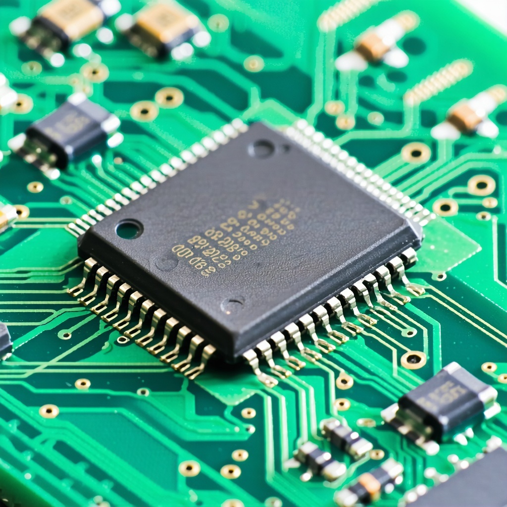
Surface Mount Technology (SMT) is a method for producing electronic circuits in which the components are mounted or placed directly onto the surface of printed circuit boards (PCBs). This technique contrasts with the traditional through-hole technology, where components are inserted into drilled holes on the PCB.
SMT allows for more compact and efficient designs, making it the preferred choice for modern electronics. It enables the incorporation of a higher density of components on a smaller board, which is crucial for the miniaturization of devices.
The SMT process is broken down into precise, sequential steps:
-
PCB Loading
PCBs are loaded onto the SMT line. -
Solder Paste Printing
A stencil printer applies solder cream (paste) onto the areas where components will be mounted. -
Solder Paste Inspection
Using AOI (Automated Optical Inspection) or manual inspection under a microscope, engineers verify that the paste is correctly applied. -
Component Placement
Pick-and-place machines, guided by vision systems, accurately place components onto the PCB. -
Reflow Soldering
The board enters a reflow oven, where controlled heating causes the solder to melt and bond components securely. -
Solder Joint Inspection
AOI systems or even X-ray machines are used to inspect solder joints, especially for BGA packages where joints are hidden beneath components. -
Manual Inspection
Operators perform final visual checks—often with the aid of microscopes to catch tiny misalignments or defects. -
PCB Unloading
The finished board is removed from the line for further functional testing or packaging.
Essential Equipment in Surface Mount Technology (SMT): A Detailed Overview
In modern electronics manufacturing, the Surface Mount Technology (SMT) process is supported by a wide range of highly specialized machines. Each piece of equipment in the SMT line plays a vital role in ensuring precision, repeatability, and overall product quality. Below is a detailed explanation of the key types of SMT equipment and their roles in the production process.
1. Stencil Printer (Solder Paste Printer)
The stencil printer is the first key machine in the SMT line. Its primary function is to apply solder paste precisely onto designated areas of the PCB (Printed Circuit Board) where components will be mounted. It uses a stencil (a fine metal sheet with custom-cut apertures) to control the amount and position of solder paste. Accurate solder paste application is crucial, as it directly affects the reliability of the solder joints and the overall performance of the assembled board.
2. Pick and Place Machine
This highly automated machine is responsible for placing SMT components onto the solder-pasted PCB with extreme speed and accuracy. It typically uses a robotic arm equipped with a vacuum nozzle to pick up components from reels or trays, align them using computer vision systems, and place them in exact positions on the board. Modern pick and place machines can handle thousands of components per hour, including tiny passive devices and complex integrated circuits.
3. Reflow Oven
After component placement, the PCB enters the reflow oven. This oven is designed to gradually heat the board through a carefully controlled thermal profile. The solder paste melts during the peak temperature phase and solidifies as the board cools, creating strong, permanent solder joints. Precise temperature control is essential to avoid defects such as cold joints, tombstoning, or thermal damage to sensitive components.
4. Wave Soldering Machine
Wave soldering is typically used for through-hole components but can also be applied to certain mixed-technology boards. In this process, the PCB passes over a wave of molten solder. The exposed metal leads and pads make contact with the solder wave, forming joints. While it is more common in traditional assembly, wave soldering is still relevant in power electronics and heavy-duty applications.
5. Smoke Extractor (Fume Extractor)
Soldering processes can generate fumes containing flux vapors and other potentially hazardous particles. A smoke extractor removes these fumes from the work area to ensure a safe and healthy environment for operators. These systems often include filters (such as HEPA and activated carbon) to capture particulates and neutralize gases.
6. AOI (Automated Optical Inspection) System
AOI systems use high-resolution cameras and advanced image processing algorithms to inspect PCBs at various stages of assembly. These machines check for issues such as misplaced or missing components, incorrect polarity, solder bridges, and insufficient solder. AOI plays a critical role in maintaining production yield and ensuring that only boards meeting strict quality standards move forward.
7. X-ray Inspection Machine
For certain component types, such as BGAs (Ball Grid Arrays), visual inspection is not sufficient because the solder joints are hidden underneath the package. X-ray inspection systems allow engineers to see through the PCB and components to detect hidden defects like voids, cold joints, or misalignments. X-ray inspection is especially important for applications requiring high reliability, such as aerospace, automotive, and medical devices.
8. Cleaning Machine
After soldering, it’s common for flux residues and other contaminants to remain on the PCB. A cleaning machine removes these residues using chemical solvents or deionized water, depending on the board and flux type. Clean PCBs not only look professional but are also less prone to long-term issues such as corrosion or electrical leakage, which can compromise product reliability.
Advanced Techniques for SMT Inspection
Advanced inspection techniques are essential for maintaining high-quality standards in SMT. Automated Optical Inspection (AOI) and X-ray inspection are two of the most common methods.
AOI uses cameras to capture images of the PCB and compare them to a predefined template to detect any discrepancies. X-ray inspection, on the other hand, allows for the examination of hidden solder joints and internal structures that are not visible to the naked eye, ensuring comprehensive quality control.
Outlined below are the comprehensive quality control processes implemented during the Surface Mount Technology (SMT) assembly to ensure the production of reliable and high-quality electronic circuit boards. These processes are designed to detect and address any potential defects at various stages of the SMT process, thereby enhancing the overall yield and reducing the need for costly rework.
-
Initial solder paste inspection (SPI)
-
Post-placement AOI
-
Post-reflow AOI or X-ray
-
Final manual inspection
This redundancy ensures that defects are caught early, reducing rework costs and improving yield.
The Role of Microscopy in SMT
Microscopy plays a crucial role in SMT, particularly for inspecting fine-pitch components and detecting micro-defects that are invisible to the naked eye. High-resolution microscopes enable technicians to closely examine solder joints, component placement, and potential defects.
Microscopy is also invaluable for failure analysis, allowing engineers to identify and rectify issues at the microscopic level, which can significantly improve the reliability and performance of the final product.
As electronics continue to evolve toward higher performance, greater functionality, and smaller form factors, the complexity of surface mount technology (SMT) has risen dramatically. One of the most critical tools that has grown in importance alongside these changes is the microscope. Microscopic inspection is no longer a supplementary step—it is now a vital part of modern electronics manufacturing. There are two main driving forces behind this trend: circuit miniaturization and the increased diversity and miniaturization of components such as MLCCs.
1. Circuit Miniaturization Requires Precision Inspection
Today’s PCBs are denser and more compact than ever before. Trace widths and component pitches are often measured in microns, leaving virtually no room for visual error. Manual inspection with the naked eye is no longer sufficient for detecting issues like:
-
Hairline solder bridges between ultra-fine pitch pads
-
Micro-cracks in solder joints
-
Incomplete solder wetting
-
Delamination or pad lifting at the microscopic level
High-magnification optical and digital microscopes allow technicians and quality engineers to inspect these tiny features with great accuracy. This precision is essential not only for detecting defects, but also for root-cause analysis and continuous process improvement.
2. Proliferation of Ultra-Small Components (e.g., MLCCs)
Surface mount components such as Multilayer Ceramic Capacitors (MLCCs) have significantly decreased in size over the past decade. It’s not uncommon to see components in 01005 packages (0.4 mm × 0.2 mm), which are smaller than a grain of sand. While these miniaturized components help save board space and improve electrical performance, they also introduce several challenges:
-
Placement accuracy must be within microns
-
Solder paste volume must be precisely controlled
-
Even slight misalignment or insufficient solder can lead to failures under stress
-
Visual inspection is virtually impossible without magnification
Microscopes make it possible to verify correct placement, assess solder joint quality, and identify early signs of stress or cracking that could lead to long-term reliability issues.
3. Quality Control and Reliability
As product lifecycles shorten and consumer expectations for quality increase, manufacturers are under more pressure than ever to ensure defect-free assembly. Microscopic inspection—both manual and automated—has become a standard part of Quality Control (QC) protocols in SMT. Combined with AOI and X-ray, microscopes provide a multi-layered inspection strategy that helps detect both visible and hidden defects early in the process.
Future Trends in SMT and Inspection Technologies
The future of SMT and inspection technologies is set to be shaped by advancements in automation, artificial intelligence (AI), and machine learning. These technologies are expected to enhance the precision and efficiency of the SMT process, reducing human error and increasing production speeds.


